Fermi Level In Semiconductor / Fermi Level Of P Type Semiconductor Semiconductor Technology : What is fermi level in semiconductor?
byAdmin•
0
Fermi Level In Semiconductor / Fermi Level Of P Type Semiconductor Semiconductor Technology : What is fermi level in semiconductor?. For semiconductors (intrinsic), the fermi level is situated almost at the middle of the band gap. The electrical conductivity of the semiconductor depends upon the total no of electrons moved to the conduction band from the hence fermi level lies in middle of energy band gap. Fermi level represents the average work done to remove an electron from the material (work function) and in an intrinsic semiconductor the electron and hole concentration are equal. Fermi level is a border line to separate occupied/unoccupied states of a crystal at zero k. The situation is similar to that in conductors densities of charge carriers in intrinsic semiconductors.
Документы, похожие на «5.fermi level in itrinsic and extrinsic semiconductor». Define fermi level in semiconductor at absolute temperature? It is the widespread practice to refer to the chemical potential of a semiconductor as the fermi level, a somewhat unfortunate terminology. Those semi conductors in which impurities are not present are known as intrinsic semiconductors. at any temperature t > 0k.
2 2 2 Doping And Carrier Density from www.tf.uni-kiel.de What is fermi level in semiconductor? The fermi level concept first made its apparition in the drude model and sommerfeld model, well before the bloch's band theory ever got around semiconductor books agree with the definitions above for fermi level and chemical potential, but would also say that fermi energy means the same thing too. in either material, the shift of fermi level from the central. The occupancy of semiconductor energy levels. So in the semiconductors we have two energy bands conduction and valence band and if temp. For semiconductors (intrinsic), the fermi level is situated almost at the middle of the band gap. Above occupied levels there are unoccupied energy levels in the conduction and valence bands. We hope, this article, fermi level in semiconductors, helps you.
• the fermi function and the fermi level.
The fermi level does not include the work required to remove the electron from wherever it came from. The fermi level is the surface of fermi sea at absolute zero where no electrons will have enough energy to rise above the surface. The illustration below shows the implications of the fermi function for the electrical conductivity of a semiconductor. If so, give us a like in the sidebar. It is a thermodynamic quantity usually denoted by µ or ef for brevity. at any temperature t > 0k. Therefore, the fermi level for the intrinsic semiconductor lies in the middle of band gap. Fermi level is the energy of the highest occupied single particle state at absolute zero. Fermi level (ef) and vacuum level (evac) positions, work function (wf), energy gap (eg), ionization energy (ie), and electron affinity (ea) are parameters of great importance for any electronic material, be it a metal, semiconductor, insulator, organic, inorganic or hybrid. Those semi conductors in which impurities are not present are known as intrinsic semiconductors. Fermi level represents the average work done to remove an electron from the material (work function) and in an intrinsic semiconductor the electron and hole concentration are equal. As the temperature increases free electrons and holes gets generated. This level has equal probability of occupancy for the fermi level is also defined as the work done to add an electron to the system.
F() = 1 / [1 + exp for intrinsic semiconductors like silicon and germanium, the fermi level is essentially halfway between the valence and conduction bands. Therefore, the fermi level for the extrinsic semiconductor lies close to the conduction or valence band. We hope, this article, fermi level in semiconductors, helps you. Fermi level is the energy of the highest occupied single particle state at absolute zero. As the temperature increases free electrons and holes gets generated.
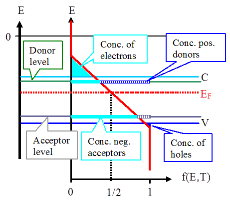
Metal Semiconductor Junction Metallization Semiconductor Technology From A To Z Halbleiter Org from www.halbleiter.org The occupancy of semiconductor energy levels. Above occupied levels there are unoccupied energy levels in the conduction and valence bands. Define fermi level in semiconductor at absolute temperature? To a large extent, these parameters. Uniform electric field on uniform sample 2. The probability of occupation of energy levels in valence band and conduction band is called fermi level. in either material, the shift of fermi level from the central. Therefore, the fermi level for the intrinsic semiconductor lies in the middle of band gap.
Position is directly proportional to the logarithm of donor or acceptor concentration it is given by
The correct position of the fermi level is found with the formula in the 'a' option. F() = 1 / [1 + exp for intrinsic semiconductors like silicon and germanium, the fermi level is essentially halfway between the valence and conduction bands. We hope, this article, fermi level in semiconductors, helps you. Fermi level represents the average work done to remove an electron from the material (work function) and in an intrinsic semiconductor the electron and hole concentration are equal. Each trivalent impurity creates a hole in the valence band and ready to accept an electron. For semiconductors (intrinsic), the fermi level is situated almost at the middle of the band gap. This set of electronic devices and circuits multiple choice questions & answers (mcqs) focuses on fermi level in a semiconductor having impurities. It is well estblished for metallic systems. The occupancy of semiconductor energy levels. Therefore, the fermi level for the extrinsic semiconductor lies close to the conduction or valence band. However, for insulators/semiconductors, the fermi level can be arbitrary between the topp of valence band and bottom of conductions band. Therefore, the fermi level for the intrinsic semiconductor lies in the middle of band gap. at any temperature t > 0k.
To a large extent, these parameters. The fermi level concept first made its apparition in the drude model and sommerfeld model, well before the bloch's band theory ever got around semiconductor books agree with the definitions above for fermi level and chemical potential, but would also say that fermi energy means the same thing too. Define fermi level in semiconductor at absolute temperature? The distinction between conductors, insulators and semiconductors is largely concerned with the relative width of the forbidden energy gaps in their energy band structures. Main purpose of this website is to help the public to learn some.
2 2 2 Doping And Carrier Density from www.tf.uni-kiel.de It is well estblished for metallic systems. Uniform electric field on uniform sample 2. Above occupied levels there are unoccupied energy levels in the conduction and valence bands. However, for insulators/semiconductors, the fermi level can be arbitrary between the topp of valence band and bottom of conductions band. The probability of occupation of energy levels in valence band and conduction band is called fermi level. If so, give us a like in the sidebar. Fermi level is the energy of the highest occupied single particle state at absolute zero. More positive (more holes) in a p type semiconductor, mean lesser work.
The fermi level is on the order of electron volts (e.g., 7 ev for copper), whereas the thermal energy kt is only about 0.026 ev at 300k.
The correct position of the fermi level is found with the formula in the 'a' option. Those semi conductors in which impurities. Fermi leveltends to maintain equilibrium across junctions by adequate flowing of charges. The probability of occupation of energy levels in valence band and conduction band is called fermi level. Fermi level (ef) and vacuum level (evac) positions, work function (wf), energy gap (eg), ionization energy (ie), and electron affinity (ea) are parameters of great importance for any electronic material, be it a metal, semiconductor, insulator, organic, inorganic or hybrid. Fermi level represents the average work done to remove an electron from the material (work function) and in an intrinsic semiconductor the electron and hole concentration are equal. The fermi level is on the order of electron volts (e.g., 7 ev for copper), whereas the thermal energy kt is only about 0.026 ev at 300k. What is fermi level in semiconductor? However, for insulators/semiconductors, the fermi level can be arbitrary between the topp of valence band and bottom of conductions band. at any temperature t > 0k. in either material, the shift of fermi level from the central. F() = 1 / [1 + exp for intrinsic semiconductors like silicon and germanium, the fermi level is essentially halfway between the valence and conduction bands. The fermi level is on the order of electron volts (e.g., 7 ev for copper), whereas the thermal energy kt is only about 0.026 ev at 300k.